Hardware
The Anne Pro contains 3 MCUs to handle each of the Keyboard, LED and BLE operations:
- Keyboard (U2) and LED (U3): STM32L151C8T6
- BLE: TI CC2541
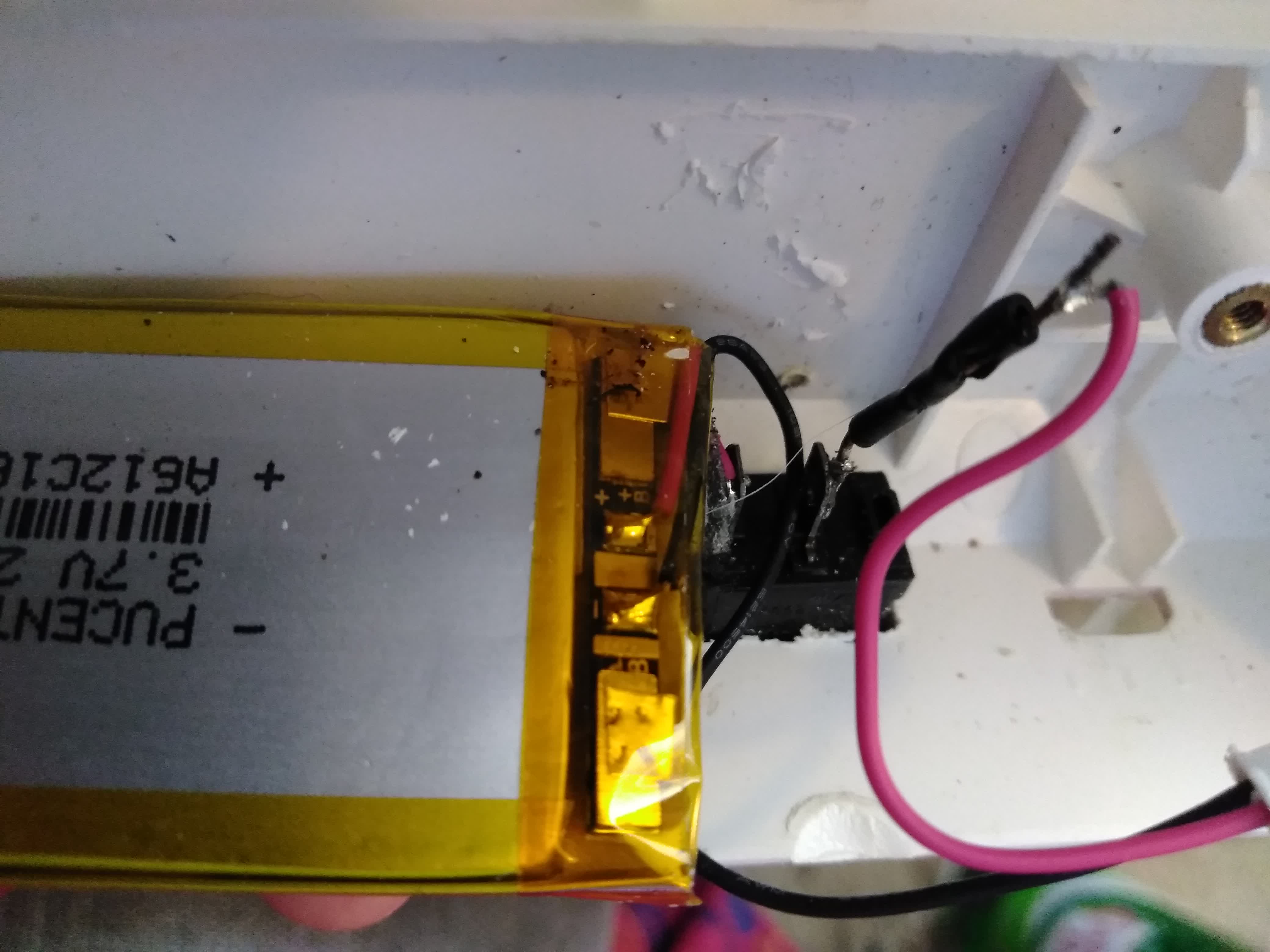
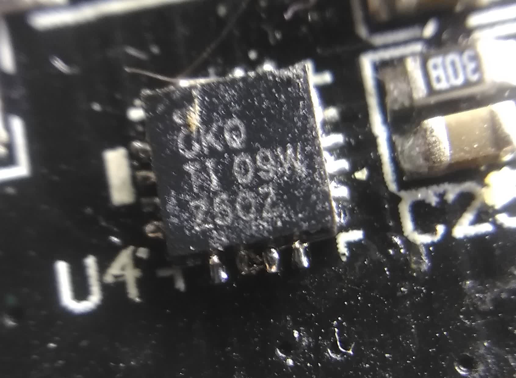
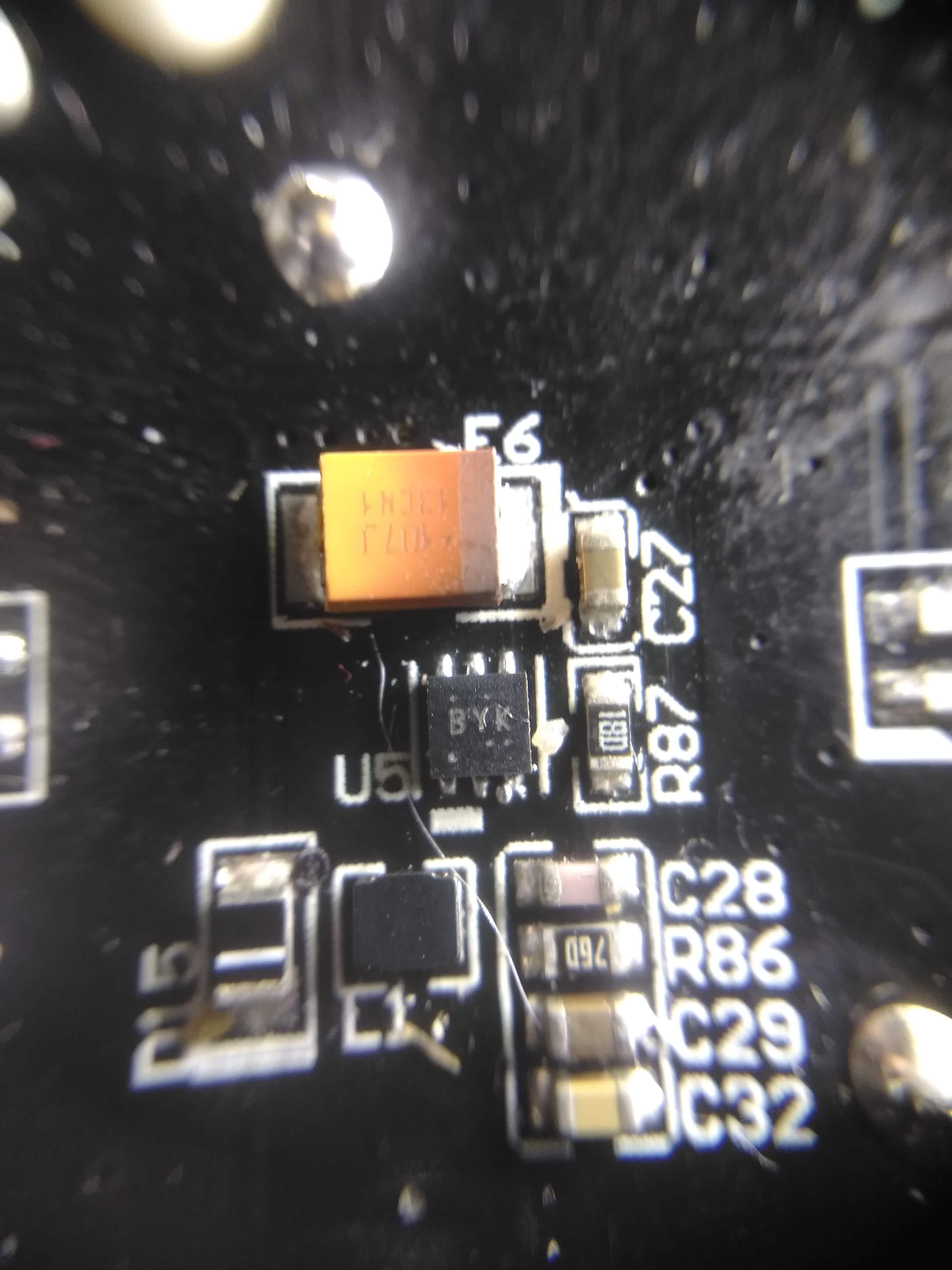
The battery circuit is managed by
- Charging chip (U4): BQ24075
(marking
CDU) or BQ24073 (markingCKQ) - Voltage step-down converter (U5):
TPS62260 (marking
BYK)
You can find some more information including pin assignments at https://github.com/hi-a/annepro-key
The STM32L151 Reference Manual and Data Sheet contain lots of useful information.
Flashing and debugging
To develop it's best to directly flash via the debug pins instead of DFU, so you get full debugging support and even working semihosting printing to your host machine.
Any ST-Link v2 or v2.1 programmer will do. You can find them cheap on ebay, or if you already have an STM32 Discovery/Nucleo board you can use the programmer built into that.
All the debug pins are exposed and easily accessible, however standard jumpers are too high for the case. You can solder on some wires and connect to your programmer:
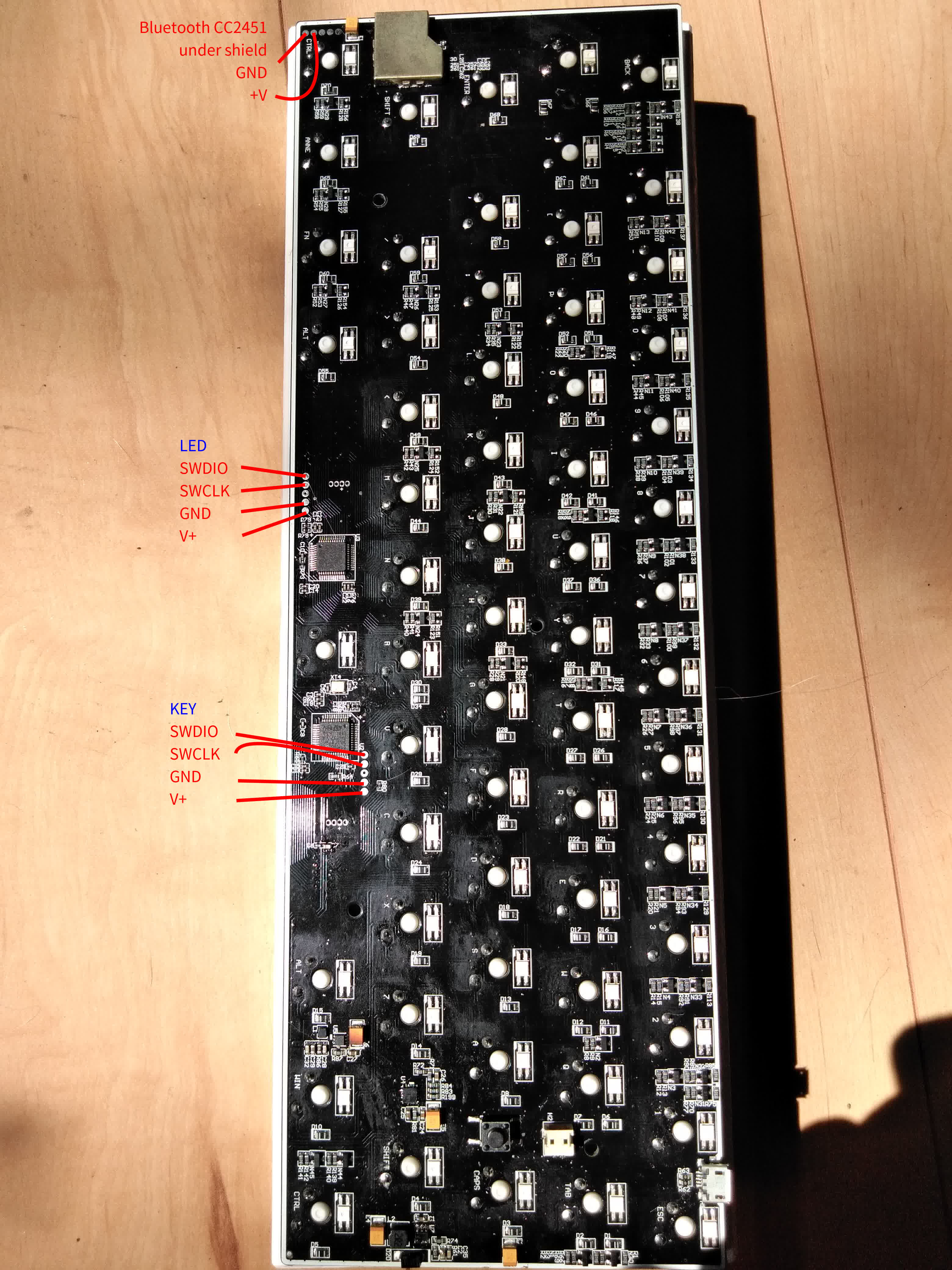
The LED chip is the one closer to the edge. The pins order is the same for both chips, counting from the BLE shield: SWDIO, SWCLK, GND, 3V3.
OpenOCD
For the best experience, use a new opencd with a unified
interface/stlink.cfg (0.11, not yet released). Otherwise you will
need to specify the precise ST-Link version in openocd.cfg. Once
your programmer is connected, make debug will build a
semihosting-enabled binary, then use arm-none-eabi-gdb and openocd
to load it into the keyboard. The semihosting output is printed to
gdb's console, and OpenOCD's messages are logged into
openocd.log. You can use another debugger by setting the GDB
variable:
env GDB=gdb-multiarch make debug
# or
make debug -e GDB=gdb-multiarch
If you like gdbgui, use make
gui-debug. However we haven't explored that tool much.
DFU
In DFU mode, the keyboard has STM's standard DFU USB identifiers
0483:DF11, with obins DFU as the product string.
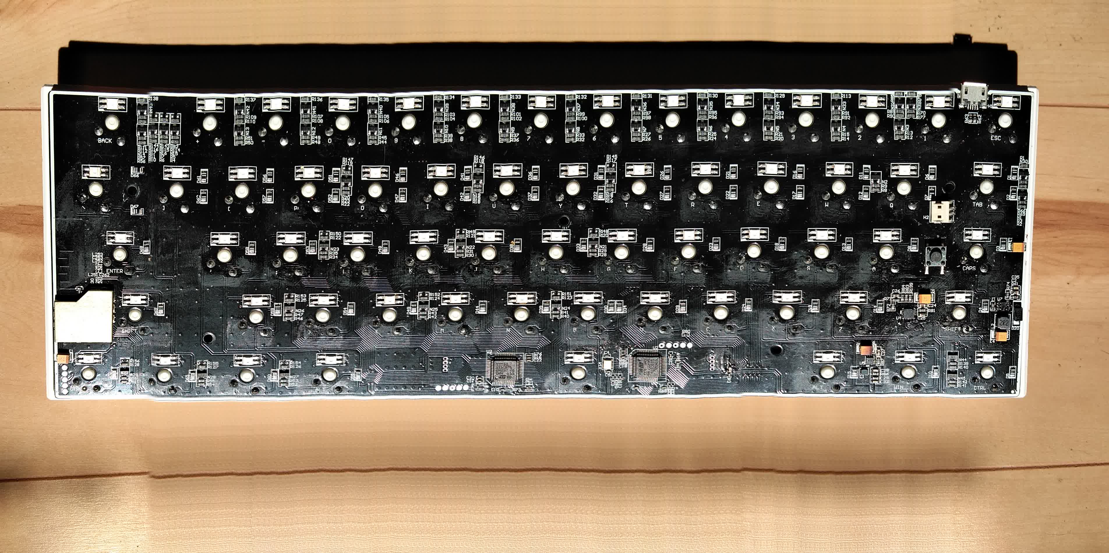
PCB Revisions
We have found two revisions, visible under the spacebar. On the switch & case color sticker by Obins, the beginning of SN is approximately your keyboard's manufacturing date.
- V2.2: earlier revision, started at least 2016-12
- Two sets of solder points under spacebar
- B31: possibly started 2017-06
- No longer has those solder points
/u/columna1 contributed excellent photos of the PCB and chips for V2.2:
Chip-to-Chip wiring
LED is on Key's PC15(for power?), communicating over USART3 by sending via DMA1 Channel2 (PB10?), receiving via DMA1 Channel3 (PB11?). BT communicate with Key over USART2, sending via DMA1 Channel7 (PA1?), receiving via DMA1 Chanel6 (PA2?), using PA3 for (?).
Keymatrix
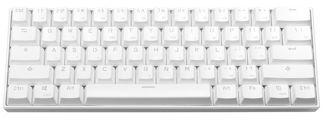
The keymatrix is connected to U2's GPIO pin groups A and B. There are 14 columns and 5 rows, giving 70 nodes. However 9 positions are not usable, marked N/a in this table.
| A5 | A6 | A7 | B0 | B1 | B12 | B13 | B14 | A8 | A9 | A15 | B3 | B4 | B5 | |
|---|---|---|---|---|---|---|---|---|---|---|---|---|---|---|
| B9 | Escape | 1 | 2 | 3 | 4 | 5 | 6 | 7 | 8 | 9 | 0 | - | = | Backspace |
| B8 | Tab | Q | W | E | R | T | Y | U | I | O | P | [ | ] | \ |
| B7 | Capslock | A | S | D | F | G | H | J | K | L | ; | ' | N/a | Enter |
| B6 | Shift | Z | X | C | V | B | N | M | , | . | / | N/a | N/a | Shift |
| A0 | Control | Meta | Alt | N/a | N/a | Space | N/a | N/a | N/a | N/a | Alt | Fn | ANNE | Control |
LED matrix
Bluetooth connection
A keyboard's L0 and L1 addresses differ only in the first hex digit. The OUI of the address can be TI, or unassigned.
Case
The PCB's screw positions are incompatible with most 60% cases.